
Electronics - Hacking the TL494 LTSpice Model#
Description#
This document provides a guide on how to hack the TL494 LTSpice model for better simulation results. It includes details on the TL494 chip, LTSpice software, and a test jig circuit for simulating the TL494’s functionality. The guide also discusses issues encountered with the original LTSpice model and how to resolve them for improved performance in simulations.
Introduction#
The TL494 is a PWM chip made by Texas Instruments. Its datasheet can be found here: http://www.ti.com/product/TL494
An important part of the design process is the ability to simulate circuits. LTSpice is an excellent SPICE simulator program provided by Linear Technology Corporation. It can be downloaded here: http://www.linear.com/designtools/software/
Unfortunately, an official LTSpice model for the TL494 chip does not exist, to my knowledge. I was able to find an unofficial LTSpice model that works fairly well here: http://www.mikrocontroller.net/topic/206248
The LTSpice files for the TL494 can be downloaded from my server here:
Place the TL494.asy file into /LTSpiceIV/lib/sym/Misc and the TL494.sub file into /LTSpiceIV/lib/sub/eigene.
The second directory must be this way or it will not work.
In the next section we will simulate with this model, discover its limitations, and discuss techniques for overcoming these limitations.
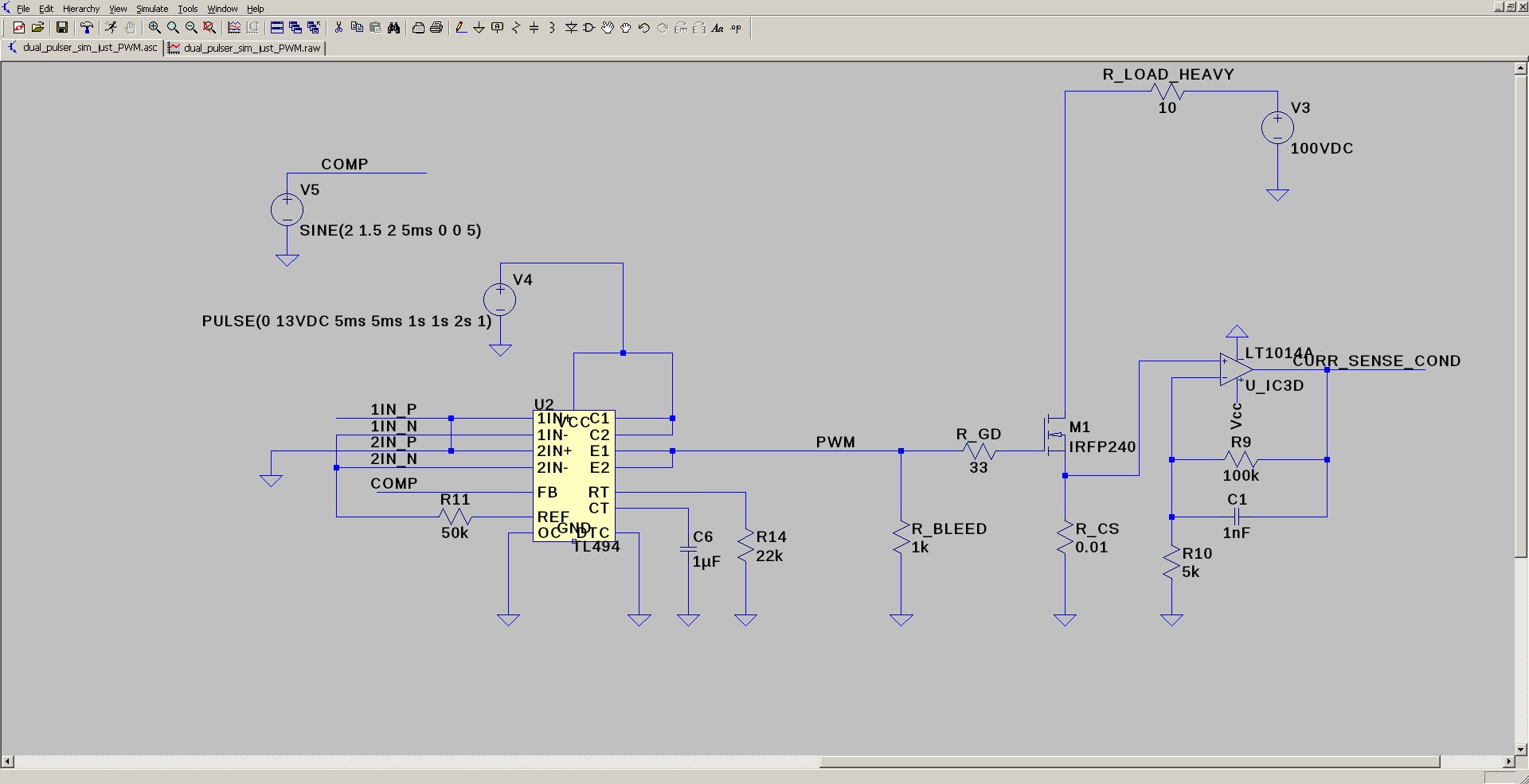
Test Jig Simulation Circuit#
There is a test jig available from the same source as the unofficial LTSpice model, but it didn’t simulate properly “out of the box.” The following test jig that I made should simulate with no issues.
Notice that the voltage source supplying Vcc is ramped up, rather than being a DC source. This allows the simulation engine to run without errors.
The error amplifiers (EA’s) are wired into max PWM configurations at the inputs, with a SIN wave source manipulating the feedback (FB) pin. The sine wave swings from a 2V offset between 3.5V and 0.5V, providing a full range of PWM duty cycle.
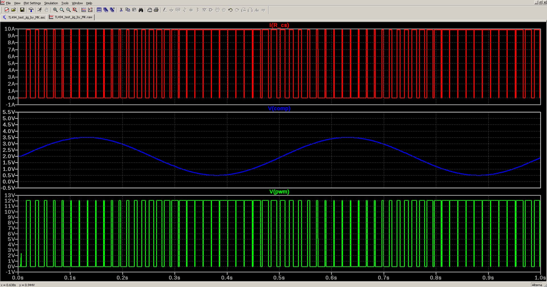
Test Jig Simulation Run#
After running the simulation of the test jig circuit, you get the following output. I placed voltage and current markers at nodes of significance, such as the PWM output and sense resistor current.
TL494 LTSpice Model Text and Issues Discussion#
When I first used the TL494 LTSpice model, I noticed that the voltage at the PWM outputs went only up to 4.8V, despite having 13V at the VCC pin.
This didn’t make sense since the saturation voltage of the internal transistors was only 2.5V maximum according to the datasheet. So I would expect at least a 10.5V PWM output. 4.8V is fine for logic-level MOSFETs, but not enough to fully enhance standard MOSFETs.
The model therefore had to be tweaked. Below is the original model text from the TL494.sub file:
* TL494.asc
*              1    2   3   4  5  6   7  8  9  10 11 12  13  14  15   16
.subckt tl494 1IN+ 1IN- FB DTC CT RT GND C1 E1 E2 C2 VCC OC REF 2IN- 2IN+
XEA1 1IN+ 1IN- VCC 0 N015 level.2 Avol=1e5 GBW=1Meg Slew=10k ilimit=25m rail=0 Vos=0 phimargin=45 en=0 enk=0 in=0 ink=0 Rin=1Meg
XEA2 2IN+ 2IN- VCC 0 N016 level.2 Avol=1e5 GBW=1Meg Slew=10k ilimit=25m rail=0 Vos=0 phimargin=45 en=0 enk=0 in=0 ink=0 Rin=1Meg
VDT N007 DTC 0.12
V2 N014 CT 0.7
A1 0 N005 0 N011 0 0 N009 0 OR vhigh=4.8 td=50n
A2 0 N006 0 N009 0 N002 0 0 OR vhigh=4.8 td=50n
A3 0 N010 0 N009 0 N012 0 0 OR vhigh=4.8 td=50n
A4 0 OC` 0 N008 0 0 N006 0 AND vhigh=4.8 td=50n
A5 0 N004 0 OC` 0 0 N010 0 AND vhigh=4.8 td=50n
E1 OC` 0 OC 0 1
A6 N004 0 N009 N001 0 N004 N008 0 DFLOP vhigh=4.8 vlow=0.2 td=50n
I2 FB 0 0.7m
R1 N003 N002 470
R2 N013 N012 470
R4 N003 E1 2k7
R5 N013 E2 2k7
Q3 RT RT Ref 0 PNP
Q4 CT RT Ref 0 PNP
S1 0 CT ctl 0 SW off
A10 CT 0 0 0 0 0 ctl 0 SCHMITT vhigh=1 vlow=-1 vt=1.5 vh=1.495 td=10n tripdt=1n
R3 VCC Ref 270
R6 N001 0 470
C1 N001 VCC 1n
XU1 N007 CT VCC 0 N005 level.2 Avol=1G GBW=1G Slew=1G ilimit=25m rail=0 Vos=0 phimargin=45 en=0 enk=0 in=0 ink=0 Rin=500Meg
XU2 FB N014 VCC 0 N011 level.2 Avol=1G GBW=1G Slew=1G ilimit=25m rail=0 Vos=0 phimargin=45 en=0 enk=0 in=0 ink=0 Rin=500Meg
Q1 C1 N003 E1 0 NPN
Q2 C2 N013 E2 0 NPN
D3 0 Ref DZ
D1 N016 FB D
D2 N015 FB D
D4 N001 VCC D
D5 0 N001 D
.model D D
.model NPN NPN
.model PNP PNP
.model sw sw(ron=1)
.lib ltc.lib
.model dz d(vrev=5)
.lib UniversalOpamps2.sub
.ends tl494
The bases of the BJT output transistors Q1 and Q2 connect to nodes N003 and N013 respectively, which are tied through 470Ω resistors (R1 and R2) to logic functions A2 and A3.
These functions have a vhigh of 4.8V, which limits the PWM output to that voltage.
Solution to the TL494 LTSpice Model Issue#
To fix the issue of the PWM output voltage being limited to 4.8V, I needed to increase the voltage at the bases of the output transistors Q1 and Q2. The original model used logic gates A2 and A3 to control the bases, which limited the output voltage to 4.8V.
Initially, I tried increasing vhigh of A2 and A3 from 4.8V to 13V, but it did not work.
Instead, I inserted 100Ω resistors and E elements with gain 2.1875 V/V between the logic gates and the transistor bases. This yielded 4.8V × 2.1875 = 10.5V, suitable for standard MOSFETs.
Note
The output voltage is fixed at 10.5V and does not simulate current-dependent saturation voltage. This is a limitation of the model.
The 100 ohm resistors were required by the simulation engine to isolate the logic elements A2 and A3 from the E elements E1000 and E1001.
Repaired model:
* TL494.asc
*              1    2   3   4  5  6   7  8  9  10 11 12  13  14  15   16
.subckt tl494 1IN+ 1IN- FB DTC CT RT GND C1 E1 E2 C2 VCC OC REF 2IN- 2IN+
XEA1 1IN+ 1IN- VCC 0 N015 level.2 Avol=1e5 GBW=1Meg Slew=10k ilimit=25m rail=0 Vos=0 phimargin=45 en=0 enk=0 in=0 ink=0 Rin=1Meg
XEA2 2IN+ 2IN- VCC 0 N016 level.2 Avol=1e5 GBW=1Meg Slew=10k ilimit=25m rail=0 Vos=0 phimargin=45 en=0 enk=0 in=0 ink=0 Rin=1Meg
VDT N007 DTC 0.12
V2 N014 CT 0.7
A1 0 N005 0 N011 0 0 N009 0 OR vhigh=4.8 td=50n
A2 0 N006 0 N009 0 N002 0 0 OR vhigh=4.8 td=50n
A3 0 N010 0 N009 0 N012 0 0 OR vhigh=4.8 td=50n
A4 0 OC` 0 N008 0 0 N006 0 AND vhigh=4.8 td=50n
A5 0 N004 0 OC` 0 0 N010 0 AND vhigh=4.8 td=50n
E1 OC` 0 OC 0 1
A6 N004 0 N009 N001 0 N004 N008 0 DFLOP vhigh=4.8 vlow=0.2 td=50n
I2 FB 0 0.7m
R1 N003 N002 470
R2 N013 N012 470
R4 N003 E1 2k7
R5 N013 E2 2k7
Q3 RT RT Ref 0 PNP
Q4 CT RT Ref 0 PNP
S1 0 CT ctl 0 SW off
A10 CT 0 0 0 0 0 ctl 0 SCHMITT vhigh=1 vlow=-1 vt=1.5 vh=1.495 td=10n tripdt=1n
R3 VCC Ref 270
R6 N001 0 470
C1 N001 VCC 1n
XU1 N007 CT VCC 0 N005 level.2 Avol=1G GBW=1G Slew=1G ilimit=25m rail=0 Vos=0 phimargin=45 en=0 enk=0 in=0 ink=0 Rin=500Meg
XU2 FB N014 VCC 0 N011 level.2 Avol=1G GBW=1G Slew=1G ilimit=25m rail=0 Vos=0 phimargin=45 en=0 enk=0 in=0 ink=0 Rin=500Meg
Q1 C1 N1010 E1 0 NPN
Q2 C2 N1011 E2 0 NPN
E1000 N1000 0 N003 0 2.1875
E1001 N1001 0 N013 0 2.1875
R1000 N1000 N1010 100
R1001 N1001 N1011 100
D3 0 Ref DZ
D1 N016 FB D
D2 N015 FB D
D4 N001 VCC D
D5 0 N001 D
.model D D
.model NPN NPN
.model PNP PNP
.model sw sw(ron=1)
.lib ltc.lib
.model dz d(vrev=5)
.lib UniversalOpamps2.sub
.ends tl494
Download the repaired model here: TL494_repaired.sub
Conclusion#
In this guide, we explored how to hack the TL494 LTSpice model to achieve better simulation results. By understanding the limitations of the original model and making necessary adjustments, we were able to simulate the TL494’s functionality more accurately.